Electronics Industry - Propharmabi

Electronics

Electronics

Cleanrooms are used in numerous processes within the electronics industry, from silicon wafer and semiconductor production to photolithography and the assembly of components such as sensors and actuators; as well as in research and development processes for the experimentation of new materials and devices. These are delicate and complex sectors that require high quality standards and a reliable partner like Propharmabi. Much of modern electronics is solid-state, meaning it is based on semiconductors made from materials such as silicon, gallium arsenide, and germanium. 
 
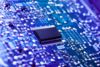
Thanks to their electrical conductivity properties, these materials have enabled the construction of increasingly smaller and more efficient components, such as the modern chips and sensors found in all the technologies we use daily: computers, smartphones, smartwatches, televisions, cameras, vehicles, and smart home appliances. 
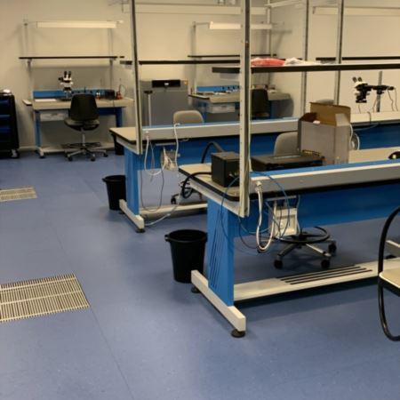
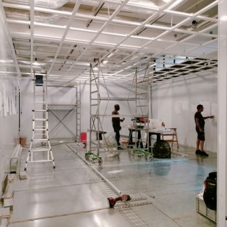
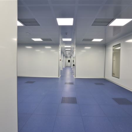
The production of these devices often involves the processing of extremely small components that must be protected from any contamination: even the smallest particles can cause failures, defects, and short circuits in the objects that have revolutionized our lives, rendering them unusable. 
 
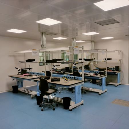
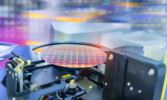
Cleanroom applications in the electronics sector range from the production of silicon wafers and semiconductors to SMT (Surface Mounted Technology) assembly of electronic components on printed circuit boards (PCBs), to the production of solar cells used to create electronic devices that capture sunlight and convert it into electricity. 
 
At Propharmabi, we apply all necessary technical standards to ensure that products meet the highest parameters of quality and reliability. In PCB manufacturing, for example, IPC standards (Institute for Printed Circuits), developed by the Association Connecting Electronics Industries, represent a set of internationally recognized guidelines and technical specifications. These standards define the geometric characteristics, materials, production processes, and acceptance criteria for PCBs, ensuring quality, interchangeability, and full compatibility among products from different manufacturers.
Electronics - Propharmabi

Areas of Intervention

  • Facilities for microchip and semiconductor production (electronic chips and photolithography)
  • Facilities for printed circuit board (PCB) assembly
  • Laboratories for testing electronic devices (optical sensors and photovoltaic devices)
  • Facilities for optical fiber production
  • Facilities for manufacturing solid-state devices and memory devices (flash memories and SSDs)
  • UV-sensitive processes
  • EUV research
  • Vacuum coating
  • Printing and assembling devices on thin surfaces


Reference Standards 

The main international reference is the ISO 14644 series.

Our work in the Electronics industry

Propharmabi's works in the electronics industry